Version. 1.12
YAMAHA
LSI
| YM2610 |
| Application Manual |
| OPNB 6-ch,4-OP.FM + SSG + ADPCM sound generator |
| 1995/1/20 |
YM2610

FM Operator Type-NB(OPNB)
■ Summary
                OPNBは、FM音源方式を採用することにより、新しいタイプのシンセサイザーとしての
                威力をもち、あらゆる音に対応することができます。 Additionally, it can be easily
                connected to a microcomputer or microprocessor, and contains built-in
                registers for storing tone information.
                さらにOPNBは、FM方式の音源とは異なった矩形波の音源およびnoise発生器に加えて
                ADPCM音源部が内蔵されています。
■ Features
                ●FM方式の音源を採用し、4音同時発生が可能であり、4音をそれぞれ異色音にす
                  ることができる。
● 4 sounds, 1 of which can be complex sine wave speech synthesis
● Two built-in programmable timers
● Built-in LFO functionality
● In addition to FM synthesis and SSG (square wave generation), ADPCM output is possible.
●FM音源部及びADPCM-A音源と同B音源にLR出力制御機能あり
● Nch-Si Gate MOS LSI
● 5V single power supply
● 64 pins
1. Summary
                OPNB has two types of ADPCM output, LR出力を可能にしたものであり主な
                Features:
                1.FM tone generator  4 channels
                2.Additional LFO functions
                3.Left/Right Output
                4.ADPCM-A tone generator    ・6 channel polyphony
                                            ・External Memory  Bankswitching up to 16 MB
                5.ADPCM-B tone generator    ・1 channel
                                            ・Variable Sampling Rate
                                              (1.8KHz~55.5KHz)
                                            ・External Memory  最大連続16MBまで可能
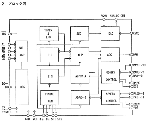
3. Major Functions
(a) FM tone generator
                    Channels          :  4
                    Operators         :  4
                    Algorithms        :  8
                    LFO function      :  Amplitude, Frequency Modulation, Modulation Existence,
                                         LFO Freqency can be set.
                    複合 Sine Wave Speech Synthesis  :  4音中1音可能
                    Timers            :  Type A, Type B
                    LR Output Control :  Can be controlled by On/Off
                    Compatible DAC    :  YM3016 (16 pins)
(B) SSG tone generator
                    Polyphony         :  3 Square Waves and White Noise
                    Analog Output     :  Converted to analog by built-in DAC,
                                         then the output is mixed to 1 terminal.
(c) ADPCM-A tone generator
                    ADPCM-A bit depth :  4 bits
                    Channels          :  6
                    Sampling Rate     :  18.5KHz
                    Sound Data ROM    :  外部ROMにより最大連続1Mバイト/6音
                                         Up to 16MB possible with bank switching
                    Start Address     :  外部より設定可能  Resolution 256 bytes
                    End Address       :  外部より設定可能  Resolution 256 bytes
                    Key On, Dump      :  Event-driven
                    Channel Level     :  Can be controlled for each channel
                    Output Level      :  Can control the level of all channels at the same time
                    LR Output Control :  Can be controlled by On/Off
(B) ADPCM-B tone generator
                    ADPCM-B bit depth :  4 bits
                    Channels          :  1
                    Sampling Rate     :  1.8~55.5KHz
                    Sound Data ROM    :  外部ROMにより最大連続16Mバイトまで可能
                    Start Address     :  外部より設定可能  Resolution 256 bytes
                    End Address       :  外部より設定可能  Resolution 256 bytes
                    Linear interpolation rate        :  55.5KHz
                    Output Level      :  Controllable
                    Repeat Play       :  Possible
                    LR Output Control :  Can be controlled by On/Off
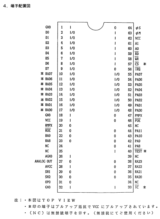
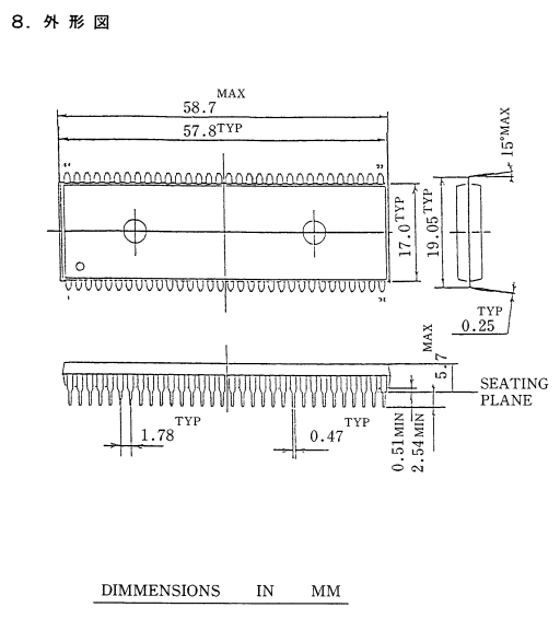
5. Pin Description
Φm (I) : Master Clock. 8MHz.
Φs,SH1,SH2 (I) : DA Converter Clock (Φs) and Synchronization Signals (SH1,SH2).
OP0 (I) : FM, ADPCM-A, ADPCM-B serial data output.
      D0~D7      (I/O) : 8bit bi-directional data bus. プロセッサとデータのやり取りをします。
      __ __ __
      CS,RD,WR,A1,A0(I) : D0~D7 data bus control. (See next page)
      ___
      IRQ           (O) : Interrupt signal. Open drain output.
ANALOG OUT (O) : SSG部のanalog出力です。ソースフォロワ出力。
RAD0~RAD7 (I/O) : ADPCM-A音源用ROMアドレス出力及びROMからのデータ入力です。
RA8~RA9 (O) : ADPCM-A sound ROM address output.
RA20~RA23 (O) : ADPCM-A sound ROM bankswitching.
      RMPX          (O) : ADPCM-A sound ROM address (lower 10 bits, upper 10 bits) latch.
      ___
      ROE           (O) : ADPCM-A音源用ROMのアウトプットイネーブル用です。
PAD0~PAD7 (I/O) : ADPCM-B音源用ROMのアドレス出力及びROMからのデータ入力です。
PA8~PA11 (O) : ADPCM-B音源用ROMのアドレス出力です。
      PMPX          (O) : ADPCM-B sound ROM address (lower 12 bits, upper 12 bits) latch.
      ___
      POE           (O) : ADPCM-B音源用ROMのアウトプットイネーブル用です。
      __
      IC            (I) : Initialization input.
      ____
      TEST          (I) : Test input.
GND,AGND (I) : Ground pin.
VCC,AVCC (I) : +5V power supply pin.
■ Data Bus Control
                                                                            __
  レジスタのアドレスやデータのリード、ライトなどのデータバスコントロールは、CS,
  __  __
  RD, WR, A1 ,A0の各信号で行います。
 __________________________________________________________________________
| __ | __ | __ |    |    |            |                                    |
| CS | RD | WR | A1 | A0 | Addr.Range |         Description                |
|____|____|____|____|____|____________|____________________________________|
|    |    |    |    |    |            |                                    |
|    |    |    |    |    | $00 - $28  |  SSG,Timer,ADPCM-B,etc. addr. write|
|  0 |  1 |  0 |  0 |  0 |____________|____________________________________|
|    |    |    |    |    |            |                                    |
|    |    |    |    |    | $30 - $B6  |  FM channel 1,2 address write      |
|____|____|____|____|____|____________|____________________________________|
|    |    |    |    |    |            |                                    |
|    |    |    |    |    | $00 - $28  |  SSG,Timer,ADPCM-B,etc. data write |
|  0 |   1|   0|   0|   1|____________|____________________________________|
|    |    |    |    |    |            |                                    |
|    |    |    |    |    | $30 - $B6  |  FM channel 1,2 data write         |
|____|____|____|____|____|____________|____________________________________|
|    |    |    |    |    |            |                                    |
|    |    |    |    |    | $00 - $2D  |  ADPCM-A address write             |
|   0|   1|   0|   1|   0|____________|____________________________________|
|    |    |    |    |    |            |                                    |
|    |    |    |    |    | $30 - $B6  |  FM channel 3,4 address write      |
|____|____|____|____|____|____________|____________________________________|
|    |    |    |    |    |            |                                    |
|    |    |    |    |    | $00 - $2D  |  ADPCM-A data write                |
|   0|   1|   0|   1|   1|____________|____________________________________|
|    |    |    |    |    |            |                                    |
|    |    |    |    |    | $30 - $B6  |  FM channel 3,4 data write         |
|____|____|____|____|____|____________|____________________________________|
|    |    |    |    |    |            |                                    |
|   0|   0|   1|   0|   0|    $XX     |  Status 0 data read                |
|____|____|____|____|____|____________|____________________________________|
|    |    |    |    |    |            |                                    |
|   0|   0|   1|   0|   1| $00 - $0D  |  SSG data read                     |
|____|____|____|____|____|____________|____________________________________|
|    |    |    |    |    |            |                                    |
|   0|   0|   1|   1|   0|    $XX     |  Status 1 data read                |
|____|____|____|____|____|____________|____________________________________|
|    |    |    |    |    |            |                                    |
|   1|   X|   X|   X|   X|    $XX     |  D0-D7 is high impedance           |
|____|____|____|____|____|____________|____________________________________|
6. Electrical Characteristics
   1. Absolute Maximum Rating
          _____________________________________________________
         |                          |                 |        |
         |    Item                  |   Rated Value   | Units  |
         |__________________________|_________________|________|
         |                          |                 |        |
         | Terminal Voltage         |     -0.3~7.0   |   V    |
         | Operating Ambient Temp.  |      0~70      |   ℃   |
         | Storage Temp.            |     -50.125     |   ℃   |
         |__________________________|_________________|________|
   2. Recommended operating conditions
          ______________________________________________________________________
         |               |          |          |          |          |          |
         |   Item        |  Symbol  |  Minimum | Standard | Maximum  |  Units   |
         |_______________|__________|__________|__________|__________|__________|
         |               |          |          |          |          |          |
         |  Power supply |   Vcc    |  4.75    |   5.0    |  5.25    |    V     |
         |       voltage |   GND    |  0       |   0      |  0       |    V     |
         |_______________|__________|__________|__________|__________|__________|
   3. DC Characteristics               ( Vcc=5v±5%, Too=0~70℃ )
         _____________________________________________________________________________________
        |                                    |         |             |        |        |      |
        |             I  t  e  m           |  Symbol |  Conditions  | Minimum | Maximum | Unit |
        |____________________________________|_________|_____________|________|________|______|
        |                  |                 |         |             |        |        |      |
        | Input High Level Voltage | All Inputs      |  VIH    |             |   2.0  |  Vcc   |  V  |
        |__________________|_________________|_________|_____________|________|________|______|
        |                  |                 |         |             |        |        |      |
        | Input Low Level Voltage  | All Inputs      |  VIL    |             |  -0.3  |    0.8 |  V  |
        |__________________|_________________|_________|_____________|________|________|______|
        |                  |                 |         |             |        |        |      |
        | クロック入力         | φM             |  VCH    |             |   2.0  |  Vcc   |  V  |
        |     HighLevel電圧 |                 |         |             |        |        |      |
        |__________________|_________________|_________|_____________|________|________|______|
        |                  |                 |         |             |        |        |      |
        | クロック入力         | φM             |  VCL    |             |  -0.3  |    0.8 |  V  |
        |     LowLevel電圧  |                 |         |             |        |        |      |
        |__________________|_________________|_________|_____________|________|________|______|
        |                  |     __ __       |         |             |        |        |      |
        | 入力リーク電圧      | φM,WR,RD,A0,A1 |  IL     |  VIN=0~5V  | -10    |   10   |  μA |
        |__________________|_________________|_________|_____________|________|________|______|
        |                  |                 |         |             |        |        |      |
        | スリーステート入力電源  | D0~D7          |  ITSL   |  VIN=0~5V  | -10    |   10   |  μA |
        |        (オフ状態)  |                 |         |             |        |        |      |
        |__________________|_________________|_________|_____________|________|________|______|
        |                  | ___             |         |             |        |        |      |
        | 出力HighLevel電圧 | IRQを除く出力   |  VOH    |  IOH=0.4mA  |   2.4  |        |  V  |
        |__________________|_________________|_________|_____________|________|________|______|
        |                  |                 |         |             |        |        |      |
        | 出力LowLevel電圧  | 全出力          |  VOL    |  IOL=2mA    |        |    0.4 |  V  |
        |__________________|_________________|_________|_____________|________|________|______|
        |                  | ___             |         |             |        |        |      |
        | 出力リーク電圧      | IRQ             |  IOL    |  VOH=0~5V  | -10    |   10   |  V  |
        |        (オフ状態)  |                 |         |             |        |        |      |
        |__________________|_________________|_________|_____________|________|________|______|
        |                  |                 |         |             |        |        |      |
        | アナログ出力電圧    | ANALOG OUT      |  VOA    |  最大音量   |   0.8  |     1.1| Vpp  |
        |                  |                 |         |  3音同時   |        |        |      |
        |                  |                 |         |  RL=470Ω  |        |        |      |
        |__________________|_________________|_________|_____________|________|________|______|
        |                  |                 |         |             |        |        |      |
        | 電源電流         |                 | ICC     |             |        |   200  |  mA  |
        |__________________|_________________|_________|_____________|________|________|______|
        |                  |            ____ |         |             |        |        |      |
        | プルアップ抵抗      | RAD0~RAD7,TEST | RPU     |             |   60   |   600  |  kΩ |
        |                  | __ __           |         |             |        |        |      |
        |                  | IC,CS           |         |             |        |        |      |
        |__________________|_________________|_________|_____________|________|________|______|
        |                  |                 |         |             |        |        |      |
        | 入力容量         | 全入力          | CI      | f=1MHz      |        |    10  |  PF  |
        |__________________|_________________|_________|_____________|________|________|______|
        |                  |                 |         |             |        |        |      |
        | 出力容量         | 全出力          | CO      |             |        |    10  |  PF  |
        |__________________|_________________|_________|_____________|________|________|______|
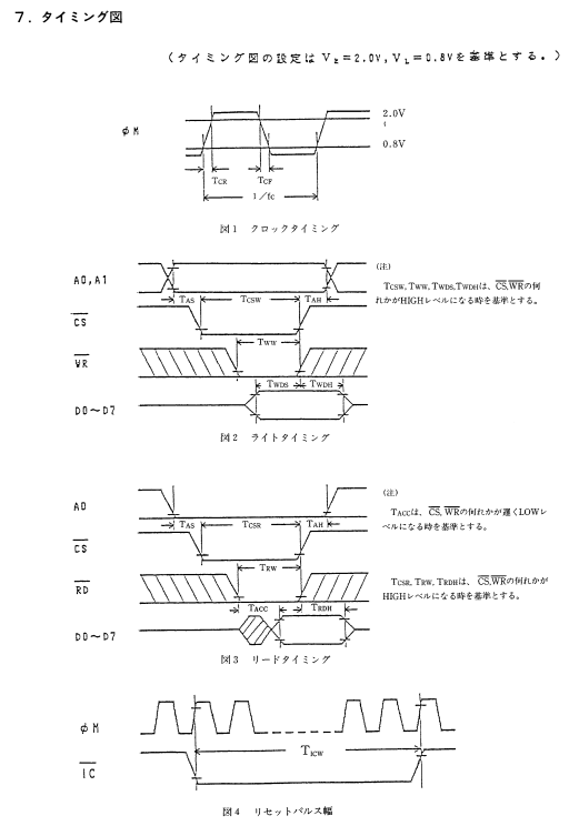
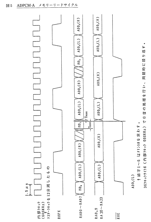
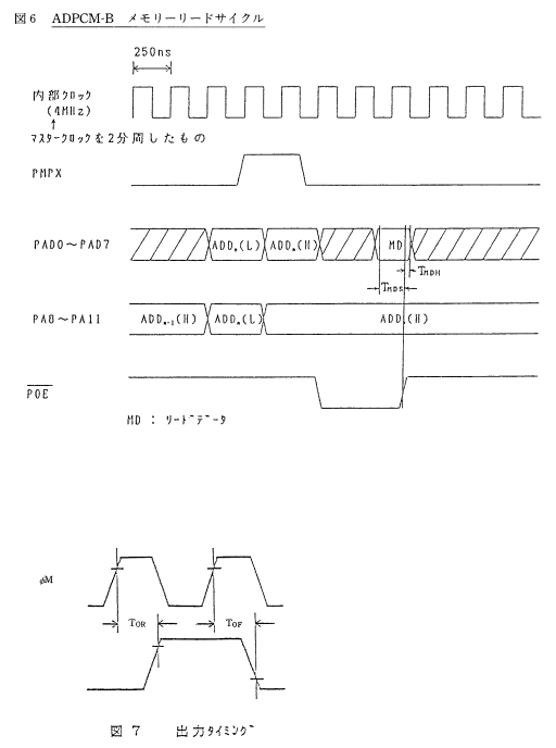
   4. AC Characteristics
  ____________________________________________________________________________________________
 |                                    |         |                 |      |      |      |      |
 |             項        目           |  記  号 |    条     件    | 最小 | 標準 | 最大 | 単位 |
 |____________________________________|_________|_________________|______|______|______|______|
 |                       |            |         |                 |      |      |      |      |
 | 入力クロック周波数        | φM        |  fc     |(Fig.1)         |   7.5|  8.0 |   8.5|  MHz |
 |_______________________|____________|_________|_________________|______|______|______|______|
 |                       |            |         |                 |      |      |      |      |
 | 入力クロックデューティ        | φM        |         |                 |  40  |  50  |  60  |  %  |
 |_______________________|____________|_________|_________________|______|______|______|______|
 |                       |            |         |                 |      |      |      |      |
 | 入力クロック立上り時間    | φM        | TCR     |(Fig.1)         |      |      |  30  |  nS  |
 |_______________________|____________|_________|_________________|______|______|______|______|
 |                       |            |         |                 |      |      |      |      |
 | 入力クロック立下り時間    | φM        | TCF     |(Fig.1)         |      |      |  30  |  nS  |
 |_______________________|____________|_________|_________________|______|______|______|______|
 |                       |            |         |                 |      |      |      |      |
 | アドレスセットアップ時間      | A0,A1      | TAS     |(Fig.2,3)     |  10  |      |      |  nS  |
 |_______________________|____________|_________|_________________|______|______|______|______|
 |                       |            |         |                 |      |      |      |      |
 | アドレスホールド時間        | A0,A1      | TAH     |(Fig.2,3)     |  10  |      |      |  nS  |
 |_______________________|____________|_________|_________________|______|______|______|______|
 |                       | __         |         |                 |      |      |      |      |
 | チップセレクトライト幅         | CS         | TCSW    |(Fig.2)         | 380  |      |      |  nS  |
 |_______________________|____________|_________|_________________|______|______|______|______|
 |                       | __         |         |                 |      |      |      |      |
 | チップセレクトリード幅        | CS         | TCSR    |(Fig.3)         | 380  |      |      |  nS  |
 |_______________________|____________|_________|_________________|______|______|______|______|
 |                       | __         |         |                 |      |      |      |      |
 | ライトパルス幅             | WR         | TWW     |(Fig.2)         | 380  |      |      |  nS  |
 |_______________________|____________|_________|_________________|______|______|______|______|
 |                       |            |         |                 |      |      |      |      |
 | ライトデータセットアップ時間    | D0~D7     | TWDS    |(Fig.2)         |  10  |      |      |  nS  |
 |_______________________|____________|_________|_________________|______|______|______|______|
 |                       |            |         |                 |      |      |      |      |
 | ライトデータホールド時間      | D0~D7     | TWDH    |(Fig.2)         |  30  |      |      |  nS  |
 |_______________________|____________|_________|_________________|______|______|______|______|
 |                       | __         |         |                 |      |      |      |      |
 | リードパルス幅            | RD         | TRW     |(Fig.3)         |  380 |      |      |  nS  |
 |_______________________|____________|_________|_________________|______|______|______|______|
 |                       |            |         |                 |      |      |      |      |
 | リードデータアクセス時間      | D0~D7     | TACC    |(Fig.3)         |      |      |  380 |  nS  |
 |_______________________|____________|_________|_________________|______|______|______|______|
 |                       |            |         |                 |      |      |      |      |
 | リードデータホールド時間     | D0~D7     | TRDH    |(Fig.3)         |  10  |      |      |  nS  |
 |_______________________|____________|_________|_________________|______|______|______|______|
 |                       | __         |         |                 |      |      |      |      |
 | リセットパルス幅            | IC         | TICW    |(Fig.4)         | 192  |      |      | Cycle |
 |_______________________|____________|_________|_________________|______|______|______|______|
 |                       |            |         |                 |      |      |      |      |
 | メモリーデータセット時間       | PAD0~     | TMDS    |(Fig.5,6)     |  70  |      |      |  nS  |
 |                       |     PAD7   |         |                 |      |      |      |      |
 |                       | RAD0~     |         |                 |      |      |      |      |
 |                       |     RAD7   |         |                 |      |      |      |      |
 |_______________________|____________|_________|_________________|______|______|______|______|
 |                       |            |         |                 |      |      |      |      |
 | メモリーデータホールド時間     | PAD0~     | TMDH    |                 |  10  |      |      |  nS  |
 |                       |     PAD7   |         |                 |      |      |      |      |
 |                       | RAD0~     |         |                 |      |      |      |      |
 |                       |     RAD7   |         |                 |      |      |      |      |
 |_______________________|____________|_________|_________________|______|______|______|______|
 |                       |            |         |                 |      |      |      |      |
 | アウトプット立上り時間     | SH1,SH2    | TOR     |CL=100PF(Fig.7)|      |      |  300 |  nS  |
 |                       | OP0  ___   |         |                 |      |      |      |      |
 |                       | RMPX,ROE   |         |                 |      |      |      |      |
 |                       | RA8,RA9    |         |                 |      |      |      |      |
 |                       | RA20~     |         |                 |      |      |      |      |
 |                       |     RA23   |         |                 |      |      |      |      |
 |                       | RAD0~RAD7 |         |                 |      |      |      |      |
 |                       | PMPX,POE   |         |                 |      |      |      |      |
 |                       | PA8~PA11  |         |                 |      |      |      |      |
 |                       | PAD0~     |         |                 |      |      |      |      |
 |                       |     PAD7   |         |                 |      |      |      |      |
 |                       | φs        |         |                 |      |      |      |      |
 |_______________________|____________|_________|_________________|______|______|______|______|
 |                       |            |         |                 |      |      |      |      |
 | アウトプット立下り時間     | SH1,SH2    | TOF     |CL=100PF(Fig.7)|      |      |  300 |  nS  |
 |                       | OP0  ___   |         |                 |      |      |      |      |
 |                       | RMPX,ROE   |         |                 |      |      |      |      |
 |                       | RA8,RA9    |         |                 |      |      |      |      |
 |                       | RA20~     |         |                 |      |      |      |      |
 |                       |     RA23   |         |                 |      |      |      |      |
 |                       | RAD0~RAD7 |         |                 |      |      |      |      |
 |                       | PMPX,POE   |         |                 |      |      |      |      |
 |                       | PA8~PA11  |         |                 |      |      |      |      |
 |                       | PAD0~     |         |                 |      |      |      |      |
 |                       |     PAD7   |         |                 |      |      |      |      |
 |                       | φs        |         |                 |      |      |      |      |
 |_______________________|____________|_________|_________________|______|______|______|______|
9. Functional Overview (1)
(a)Register Writing
   When writing to the registers, first set the address, then send the data.
 (The order must always be address followed by data). However, if you're accessing
 the same address multiple times, you may write the address first and procceed to
 write the data register multiple times.
   After writing to the address or data registers, you must wait before accessing
 them again. The wait time differs between address and data writes.
                       Wait Time
           ____________________________________________
          |                   |                        |
          | after addr. write |       17 cycles        |
          |___________________|________________________|
          |                   |                        |
          | after data write  |       83 cycles        |
          |___________________|________________________|
The number of cycles is based on the master clock.
(B)ADPCM Register Initial Values
Cleared at initialization time(IC="0"), register initial values are as follows:
ADPCM-A ADPCM-B
ADDRESS      REGISTER        Init.Value      ADDRESS      REGISTER       Init.Value
 ____     _____________________________     ____    _____________________________
         |                  |          |           |                    |        |
  00     | DUMP/ADPCM-A ON  |   "00"   |     10    | CONTROL 1          |  "00"  |
 ____    |__________________|__________|    ____   |____________________|________|
         |                  |          |           |                    |        |
  01     | TOTAL LEVEL      |   "00"   |     11    | CONTROL 2          |  "00"  |
 ____    |__________________|__________|    ____   |____________________|________|
         |                  |          |           |                    |        |
  02     | TEST             |   "00"   |     12    | START  ADR (L)     |  "XX"  |
 ____    |__________________|__________|    ____   |____________________|________|
         |                  |          |           |                    |        |
  08     | OUTPUT SELECT    |   "00"   |     13    | START  ADR (H)     |  "XX"  |
  0D     | CHANNEL LEVEL    |          |    ____   |____________________|________|
 ____    |__________________|__________|           |                    |        |
         |                  |          |     14    | END ADR (L)        |  "XX"  |
  10     | START ADR (L)    |   "00"   |    ____   |____________________|________|
  15     |                  |          |           |                    |        |
 ____    |__________________|__________|     15    | END ADR (H)        |  "XX"  |
         |                  |          |    ____   |____________________|________|
  18     | START ADR (H)    |   "00"   |           |                    |        |
  1D     |                  |          |     19    | DELTA-N (L)        |  "XX"  |
 ____    |__________________|__________|    ____   |____________________|________|
         |                  |          |           |                    |        |
  20     | END ADR (L)      |   "00"   |     1A    | DELTA-N (H)        |  "XX"  |
  25     |                  |          |    ____   |____________________|________|
 ____    |__________________|__________|           |                    |        |
         |                  |          |     1B    | EG CONTROL         |  "XX"  |
  28     | END ADR (H)      |   "00"   |    ____   |____________________|________|
  2D     |                  |          |           |                    |        |
 ____    |__________________|__________|     1C    | FLAG CONTROL       |  "00"  |
                                            ____   |____________________|________|
"XX" = undefined
Functional Overview (2)
■ Register Address Allocation
          When A1 = 0                    When A1 = 1
    $00   __________________       $00   __________________
         |      SSG         |           |                  |
    $0F  |                  |           |                  |
    $10  |__________________|           |                  |
         |      ADPCM-B     |           |     ADPCM-A      |
    $1F  |                  |           |                  |
    $20  |__________________|           |                  |
         |      FM          |           |                  |
    $2F  |    (Common)      |      $2F  |                  |
    $30  |__________________|      $30  |__________________|
         |      FM          |           |      FM          |
         |     (CH1,CH2)    |           |     (CH3,CH4)    |
    $B6  |__________________|      $B6  |__________________|
(a) Read/Write Data(SSG)
    ADDR.     D7    D6    D5    D4    D3    D2    D1    D0              COMMENT
    _____  __________________________________________________   _______________________
          |                                                  |
     00   |                    Fine Tune                     |
          |__________________________________________________|  Channel-A Tone Period
          |                        |                         |
     01   |========================|      Coarse Tune        |
    ____  |________________________|_________________________|  _______________________
          |                                                  |
     02   |                    Fine Tune                     |
          |__________________________________________________|  Channel-B Tone Period
          |                        |                         |
     03   |========================|      Coarse Tune        |
    ____  |________________________|_________________________|  _______________________
          |                                                  |
     04   |                    Fine Tune                     |
          |__________________________________________________|  Channel-C Tone Period
          |                        |                         |
     05   |========================|      Coarse Tune        |
    ____  |________________________|_________________________|  _______________________
          |                  |                               |
     06   |==================|       Period Control          |  Noise Period
    ____  |__________________|_______________________________|  _______________________
          |           |                   |                  |
     07   |===========|      /Noise       |    /Tone         |  /Enable
    ____  |___________|___________________|__________________|  _______________________
          |                 |      |                         |
     08   |=================|  M   |         Level           |  Channel-A Amplitude
          |_________________|______|_________________________|
          |                 |      |                         |
     09   |=================|  M   |         Level           |  Channel-B Amplitude
          |_________________|______|_________________________|
          |                 |      |                         |
     0A   |=================|  M   |         Level           |  Channel-C Amplitude
    ____  |_________________|______|_________________________|  _______________________
          |                                                  |
     0B   |                    Fine Tune                     |
          |__________________________________________________|  Envelop Period
          |                                                  |
     0C   |                    Coarse tune                   |
    ____  |__________________________________________________|  _______________________
          |                         |     |     |     |      |
     0D   |=========================| CON | ATT | ALT | HLD  |  Envelop Shape Cycle
    ____  |_________________________|_____|_____|_____|______|  _______________________
(B) Write Data (ADPCM-B)
    ADDR.   D7  D6  D5  D4  D3  D2  D1  D0
    _____  ________________________________
          |                                |
     10   |           Control 1            |
    _____ |________________________________|
          |                                |
     11   |           Control 2            |
    _____ |________________________________|
          |                                |
     12   |           Start ADDR.(L)       |
    _____ |________________________________|
          |                                |
     13   |           Start ADDR.(H)       |
    _____ |________________________________|
          |                                |
     14   |           End ADDR.(L)         |
    _____ |________________________________|
          |                                |
     15   |           End ADDR.(H)         |
    _____ |________________________________|
          |                                |
     16   |================================|
    _____ |________________________________|
          |                                |
     17   |================================|
    _____ |________________________________|
          |                                |
     18   |================================|
    _____ |________________________________|
          |                                |
     19   |           Delta-N(L)           |
    _____ |________________________________|
          |                                |
     1A   |           Delta-N(H)           |
    _____ |________________________________|
          |                                |
     1B   |           EG Control           |
    _____ |________________________________|
          |                                |
     1C   |           Flag Control         |
    _____ |________________________________|
(c) Write Data (FM)
    ADDR.    D7  D6  D5  D4  D3  D2  D1  D0         COMMENT
    _____   ________________________________   __________________________
           |                                |
     21    |               Test             |  LSI Test Data
           |________________________________|  __________________________
           |                |               |
     22    |================|      LFO      |  LFO Freq Control
           |________________|_______________|  __________________________
           |                                |
     24    |              Timer-A           |  Timer-A upper 8 bits
           |________________________________|  __________________________
           |                       |        |
     25    |=======================|Timer-A |  Timer-A lower 2 bits
           |_______________________|________|  __________________________
           |                                |
     26    |              Timer-B           |  Timer-B Data
           |________________________________|  __________________________
           |        |       |        |      |
           |  Mode  | Reset | Enable | Load |  Timer-A/B Control and
     27    |        |  B  A |  B  A  | B  A |  2 CH Mode
           |________|_______|________|______|  __________________________
           |                |   |           |
     28    |      Slot      |===|     CH    |  Key-ON/OFF
           |________________|___|___________|  __________________________
           |                                |
    29~   |================================|
       2F  |________________________________|  __________________________
           |    |           |               |
    31~3E |====|    DT     |   MULTI       |  Detune/Multiple
           |____|___________|_______________|  __________________________
           |    |                           |
    41~4E |====|               TL          |  Total Level
           |____|___________________________|  __________________________
           |        |   |                   |
    51~5E |   KS   |===|       AR          |  Key Scale/Attack Rate
           |________|___|___________________|  __________________________
           |    |       |                   |
    61~6E | AM |=======|       DR          |  AMON/Decay Rate
           |____|_______|___________________|  __________________________
           |            |                   |
    71~7E |============|       SR          |  Sustain Rate
           |____________|___________________|  __________________________
           |                |               |
    81~8E |        SL      |     RR        |  Sustain Level/Release Rate
           |________________|_______________|  __________________________
           |                |               |
    91~9E |================|     SSG-EG    |  SSG-Type Envelop Control
           |________________|_______________|  __________________________
           |                                |
    A1,A2  |             F-Num 1            |
           |________________________________|  F-Numbers/Block
           |        |           |           |
    A5,A6  |========|    Block  |  F-Num 2  |
           |________|___________|___________|  __________________________
           |                                |
    A9,AA  |           2 CH * F-Num 1       |
           |________________________________|  2 CH - 2 Slot
           |        |           |           |  F-Numbers/Block
    AD,AE  |========| 2CH*Block | 2CH*F-Num2|
           |________|___________|___________|  __________________________
           |        |           |           |
    B1,B2  |========|    FB     |   Connect |  Self Feedback/Connection
           |________|___________|___________|  __________________________
           |    |   |        |  |           |
    B5,B6  | L  | R |   AMS  |==|    PMS    |  LR SEL./AM,PM SENS
           |____|___|________|__|___________|  __________________________
※ Internal register address use
            _________________________________
           |         |     |     |     |     |
           |   slot  |  1  |  2  |  3  |  4  |
           |_________|_____|_____|_____|_____|
           |         |     |     |     |     |
           | ch1,ch3 | *1  | *5  | *9  | *D  |
           |_________|_____|_____|_____|_____|
           |         |     |     |     |     |
           | ch2,ch4 | *2  | *6  | *A  | *E  |
           |_________|_____|_____|_____|_____|
(d) Write Data (ADPCM-A)
    ADDR.   D7   D6   D5   D4   D3   D2   D1   D0        COMMENT
    _____  _______________________________________   ______________________
          |    |    |                             |
     00   | DM |====|          AON                |  Dump/ADPCM-A ON
    _____ |____|____|_____________________________|  ______________________
          |         |                             |
     01   |=========|          ATL                |  ADPCM-A Total Level
    _____ |_________|_____________________________|  ______________________
          |                                       |
     02   |                    Test               |  LSI Test Data
    _____ |_______________________________________|  ______________________
          |    |    |     |                       |
     08   |  L | R  |=====|         AC L          |  Output Select
     0D   |    |    |     |                       |  Channel Level
    _____ |____|____|_____|_______________________|  ______________________
          |                                       |
     10   |           Start ADDR.(L)              |
     15   |                                       |
    _____ |_______________________________________|  Start Address
          |                                       |
     18   |           Start ADDR.(H)              |
     1D   |                                       |
    _____ |_______________________________________|  ______________________
          |                                       |
     20   |           End ADDR.(L)                |
     25   |                                       |
    _____ |_______________________________________|  End Address
          |                                       |
     28   |           End ADDR.(L)                |
     2D   |                                       |
    _____ |_______________________________________|  ______________________
(e) Read Data
    ADDR.                                                   COMMENT
    ______   ______________________________________   ______________________
            |                                      |
     XX     |           FLAG                       |  Status 0  (when A1="0")
            |______________________________________|  Status 1  (when A1="1")
Functional Overview (3)
■ ADPCM-A Register Functions and Descriptions
DUMP/ADPCM-A  ON  ($00)
 _________________________________________________
|      |      |                                   |
|  D7  |  D6  |  D5    D4    D3    D2    D1    D0 |
|______|______|___________________________________|
|      |      |                                   |
|  DM  |  --  |            AON                    |
|______|______|___________________________________|
DM :"1"の時音をdump, produces a sound when "0".
AON : Specify ADPCM-A channel control bits.
ADPCM-A  Total Level  ($01)
 _________________________________________________
|      |      |                                   |
|  D7  |  D6  |  D5    D4    D3    D2    D1    D0 |
|______|______|___________________________________|
|      |      |                                   |
|  --  |  --  |            ATL                    |
|______|______|___________________________________|
ATL :ADPCM-A volume is set between 0 ~ -47.25dB in steps of 0.75dB.
     all "1" equals 0 dB.
TEST ($02)
      This address is provided to test the LSI.
      Usually all "0".
Output Select/Channel Level ($08-0D)
 _________________________________________________
|      |      |                                   |
|  D7  |  D6  |  D5    D4    D3    D2    D1    D0 |
|______|______|___________________________________|
|      |      |                                   |
|  L   |  R   |                 ACL               |
|______|______|___________________________________|
L   : When "1", outputs to Left channel.
R   : When "1", outputs to Right channel.
ACL :Each channel's level is 0 ~ -23.25dB in steps of 0.75dB.
     all "1" = 0 dB
Start Addr. L/H  ($10 ~ 15/$18 ~1D)
 _______________________       _________________________        ________________
|                       |     |                         |      |                |
|  * * * * D3 D2 D1 D0  |     | D7 D6 D5 D4 D3 D2 D1 D0 |      |0 0 0 0 0 0 0 0 |
|_______________________|     |_________________________|      |________________|
\                      \    |                         |    /                /
  \   Start Address(H)   \  |    Start Address(L)     |  /   Fix Level    /
    \______________________\|_________________________|/________________/
     |                                                                    |
     | 23 22 21 20 19 18 17 16   15 14 13 12 11 10 9 8    7 6 5 4 3 2 1 0 |
     |____________________________________________________________________|
     |                                                                    |
     |                                ROM Address                         |
     |____________________________________________________________________|
End Addr. L/H  ($20 ~ 25/$28 ~ 2D)
 _______________________       _________________________        ________________
|                       |     |                         |      |                |
|  * * * * D3 D2 D1 D0  |     | D7 D6 D5 D4 D3 D2 D1 D0 |      |0 0 0 0 0 0 0 0 |
|_______________________|     |_________________________|      |________________|
\                      \    |                         |    /                /
  \    End Address(H)    \  |      End Address(L)     |  /   Fix Level    /
    \______________________\|_________________________|/________________/
     |                                                                    |
     | 23 22 21 20 19 18 17 16   15 14 13 12 11 10 9 8    7 6 5 4 3 2 1 0 |
     |____________________________________________________________________|
     |                                                                    |
     |                                ROM Address                         |
     |____________________________________________________________________|
* $18 ~ 1D's D4 ~ D7 values and $28 ~ $2D's D4 ~ D7 values must be the same.
■ADPCM-A Synthesis Process
 ____________________________________________________________________________
|            |       |                                                       |
| Address    | Data  |                        Comment                        |
|____________|_______|_______________________________________________________|
|            |       |                                                       |
|            |       | Default                                               |
|  $1C       |  $3F  |    Mask Flags A0-A5 (flag reset)                      |
|            |       |                                                       |
|            |       |                                                       |
|  $1C       |  $00  |    Enable flags                                       |
|            |       |                                                       |
|            |       |                                                       |
|  $01       |  $3F  |    Total Level setting (Maximum)                      |
|            |       |                                                       |
|            |       |                                                       |
|  $08-$0D   |  $DF  |    Channel Level setting (Maximum)                    |
|            |       |                                                       |
|            |       |                                                       |
|  $10-$15   |  $XX  |    Memory address start (L)                           |
|            |       |                                                       |
|            |       |                                                       |
|  $18-$1D   |  $XX  |    Memory address start (H)                           |
|            |       |                                                       |
|            |       |                                                       |
|  $20-$25   |  $XX  |    Memory address end (L)                             |
|            |       |                                                       |
|            |       |                                                       |
|  $28-$2D   |  $XX  |    Memory address end (H)                             |
|            |       |                                                       |
|            |       |                                                       |
|  Initalize |       |                                                       |
|  Synthesis |       |                                                       |
|            |       |                                                       |
|  $00       |  $XX  |    AONビットが "1"になるのに同期して各チャンネルの    |
|            |       |  合成開始(DM bit = "0")。                           |
|            |       |    FLAG A0-A5が "1"となり、合成を指示するまで待機。   |
|            |       |    DMビットを "1"にして AONビットを "1"にすると、その |
|            |       |    チャンネルは合成を中止する。                       |
|            |       |  End of synthesis                                     |
|            |       |    Synthesis ends when FLAG A0-A5 is "1".             |
|____________|_______|_______________________________________________________|


■ADPCM-A Sound Source
 ______________________________________________________________________
|       |         |  Output  |   Start   |    End    |          |      |
| Chan. | AON bit |  Select  |  Address  |  Address  |End Synth.| Flag |
|_______|_________|__________|___________|___________|__________|______|
|       |         |          |           |           |          |      |
|   1   |    D0   |    $08   |  $10/$18  |  $20/$28  |   FLAG   |  A0  |
|_______|_________|__________|___________|___________|__________|______|
|       |         |          |           |           |          |      |
|   2   |    D1   |    $09   |  $11/$19  |  $21/$29  |   FLAG   |  A1  |
|_______|_________|__________|___________|___________|__________|______|
|       |         |          |           |           |          |      |
|   3   |    D2   |    $0A   |  $12/$1A  |  $22/$2A  |   FLAG   |  A2  |
|_______|_________|__________|___________|___________|__________|______|
|       |         |          |           |           |          |      |
|   4   |    D3   |    $0B   |  $13/$1B  |  $23/$2B  |   FLAG   |  A3  |
|_______|_________|__________|___________|___________|__________|______|
|       |         |          |           |           |          |      |
|   5   |    D4   |    $0C   |  $14/$1C  |  $24/$2C  |   FLAG   |  A4  |
|_______|_________|__________|___________|___________|__________|______|
|       |         |          |           |           |          |      |
|   6   |    D5   |    $0D   |  $15/$1D  |  $25/$2D  |   FLAG   |  A5  |
|_______|_________|__________|___________|___________|__________|______|
Functional Overview (4)


■ADPCM-B Register Functions and Descriptions

Control 1  ($10)
 ______________________________
|                              |
| D7 D6 D5 D4 D3 D2 D1 D0      |
|______________________________|
|                              |
| START - - REPEAT - - - RESET |
|______________________________|


ADPCM-B Start, Control external memory access

RESET  : 実行中に"1"とすると初期状態に戻る。但し、REPEATは"0"。
REPEAT : When "1", repeats ADPCM-B output from the same addresses.
START  : When "1", ADPCM-B output begins.


Control 2  ($11)
 _________________________
|                         |
| D7 D6 D5 D4 D3 D2 D1 D0 |
|_________________________|
|                         |
| L R - - - - - -         |
|_________________________|

L : When "1", output to Left channel
R : When "1", output to Right channel

Start Address L/H  ($12/$13)
 ____________________________       _________________________        ________________
|                            |     |                         |      |                |
|   D7 D6 D5 D4 D3 D2 D1 D0  |     | D7 D6 D5 D4 D3 D2 D1 D0 |      |0 0 0 0 0 0 0 0 |
|____________________________|     |_________________________|      |________________|
\                           \    |                         |    /                /
  \   Start Address(H)        \  |    Start Address(L)     |  /   Fix Level    /
    \___________________________\|_________________________|/________________/
     |                                                                         |
     |  23 22 21 20 19 18 17 16      15 14 13 12 11 10 9  8    7 6 5 4 3 2 1 0 |
     |_________________________________________________________________________|
     |                                                                         |
     |                                ROM Address                              |
     |_________________________________________________________________________|

End Address L/H  ($14/$15)
 ___________________________        _________________________        ________________
|                           |      |                         |      |                |
|  D7 D6 D5 D4 D3 D2 D1 D0  |      | D7 D6 D5 D4 D3 D2 D1 D0 |      |0 0 0 0 0 0 0 0 |
|___________________________|      |_________________________|      |________________|
\                           \    |                         |    /                /
  \    End Address(H)         \  |      End Address(L)     |  /   Fix Level    /
    \___________________________\|_________________________|/________________/
     |                                                                         |
     |  23 22 21 20 19 18 17 16      15 14 13 12 11 10 9  8    7 6 5 4 3 2 1 0 |
     |_________________________________________________________________________|
     |                                                                         |
     |                                ROM Address                              |
     |_________________________________________________________________________|
Delta-N L/H  ($19/$1A)
 ____________________________             ___________________________
|                            |           |                           |
|   D7 D6 D5 D4 D3 D2 D1 D0  |           |  D7 D6 D5 D4 D3 D2 D1 D0  |
|____________________________|           |___________________________|
|                            \        /                            |
|     DELTA-N (H)              \    /         DELTA-N (L)          |
|________________________________\/________________________________|
|                                 ||                                 |
| d15 d14 d13 d12 d11 d10  d9  d8 || d7  d6   d5  d4  d3  d2  d1  d0 |
|_________________________________||_________________________________|
|                                                                    |
|                              DELTA-N                               |
|____________________________________________________________________|
The sampling rate for ADPCM-B is specified like so:
           △N
      f. = ――  *  55.5   [KHz]
           256
(Translator's note: The original document I translated had division by 216.)
EG Control  ($1B)
    ___________________________
   |                           |
   |  D7 D6 D5 D4 D3 D2 D1 D0  |
   |___________________________|
   |                           |
   |        EG-Control         |
   |___________________________|
ADPCM-B Output Level Control
all "1" = max
Flag Control  ($1C)
 _______________________________________________________________________
|        |        |        |        |        |        |        |        |
|   D7   |   D6   |   D5   |   D4   |   D3   |   D2   |   D1   |   D0   |
|________|________|________|________|________|________|________|________|
|        |        |        |        |        |        |        |        |
|  MSK   |        |   MSK  |   MSK  |   MSK  |   MSK  |   MSK  |   MSK  |
|   B    |   _    |   A5   |   A4   |   A3   |   A2   |   A1   |   A0   |
|________|________|________|________|________|________|________|________|
ADPCM Flag Control
When MSK bit = "1", the corresponding flag in Status 1 is "0".
■ADPCM-B Synthesis Process
 _____________________________________________________________________
|       |       |                                                     |
| Addr. | Data  |                     Comment                         |
|_______|_______|_____________________________________________________|
|       |       |                                                     |
|       |       | Default                                             |
|  $1C  |  $80  |    Mask Flag B (Reset flags)                        |
|       |       |                                                     |
|       |       |                                                     |
|  $1C  |  $00  |    Enable flags                                     |
|       |       |                                                     |
|       |       |                                                     |
|  $10  |  $00  |    Enable ADPCM-B output                            |
|       |       |                                                     |
|       |       |                                                     |
|  $11  |  $C0  |    L and R channel output                           |
|       |       |                                                     |
|       |       |                                                     |
|  $12  |  $XX  |    Memory start address (L)                         |
|       |       |                                                     |
|       |       |                                                     |
|  $13  |  $XX  |    Memory start address (H)                         |
|       |       |                                                     |
|       |       |                                                     |
|  $14  |  $XX  |    Memory end address (L)                           |
|       |       |                                                     |
|       |       |                                                     |
|  $15  |  $XX  |    Memory end address (H)                           |
|       |       |                                                     |
|       |       |                                                     |
|  $19  |  $BA  |    Sampling Rate 16 KHz (⊿N=18874)                |
|       |       |                                                     |
|       |       |                                                     |
|  $1A  |  $49  |                                                     |
|       |       |                                                     |
|       |       |                                                     |
|  $1B  |  $FF  |    Set the output level (Maximum)                   |
|       |       |  Synthesis Initiation                               |
|       |       |                                                     |
|  $10  |  $80  |    Output begins when the START bit of register $10 |
|       | (/$90)|    is set to "1".                                   |
|       |       |  Synthesis                                          |
|       |       |    FLAG Bが "1"となり合成終了を指示するまで待機。   |
| ($10) | ($80) |    (Cancel repeat.)                                 |
| ($10) | ($01) |    (Force stop synthesis.)                          |
|       |       |  Synthesis End                                      |
|  $10  |  $00  |    Stop ADPCM-B output. Clear register $10          |
|_______|_______|_____________________________________________________|
(Translator's note: The first entry in "Sampling Rate 16 KHz was "xx". 18874 = $49BA)
Functional Overview (5)
■ LFO Register Function and Description
LFO Frequency ($22)
    ____________________________________________________________
   |                              |        |                    |
   |  D7      D6      D5      D4  |   D3   |  D2    D1     D0   |
   |______________________________|________|____________________|
   |                              |        |                    |
   |==============================| LFO ON | FREQ  CONT         |
   |______________________________|________|____________________|
    ____________________________________________________________________
   |            |      |      |      |      |      |      |      |      |
   | FREQ CONT  |   0  |   1  |   2  |   3  |   4  |   5  |   6  |   7  |
   |____________|______|______|______|______|______|______|______|______|
   |            |      |      |      |      |      |      |      |      |
   | freq (Hz)  | 3.98 | 5.56 | 6.02 | 6.37 | 6.88 | 9.63 | 48.1 | 72.2 |
   |____________|______|______|______|______|______|______|______|______|
       FREQ CONT : Value is set based on the 8 values in the above table.
       LFO ON    : When "1", LFO is on.
PMS/AMS/LR  ($B5 - $B6)
 ______________________________________________________
|      |      |              |      |                  |
|  D7  |  D6  |  D5      D4  |  D3  |  D2    D1    D0  |
|______|______|______________|______|__________________|
|      |      |              |      |                  |
|  L   |  R   |       AMS    |======|        PMS       |
|______|______|______________|______|__________________|
   PMS      : Control phase modulation (based on table below).
   AMS      : Control amplitude modulation (based on table below).
   L,R      : Specify Left/Right channel output.
 ____________________________________________________________
|            |     |     |     |     |     |     |     |     |
|     PMS    |  0  |  1  |  2  |  3  |  4  |  5  |  6  |  7  |
|____________|_____|_____|_____|_____|_____|_____|_____|_____|
|            |     |     |     |     |     |     |     |     |
|Diff.(Cents)|  0  |±3.4|±6.7|±10 |±14 |±20 |±40 |±80 |
|____________|_____|_____|_____|_____|_____|_____|_____|_____|
 ____________________________________
|            |     |     |     |     |
|     AMS    |  0  |  1  |  2  |  3  |
|____________|_____|_____|_____|_____|
|            |     |     |     |     |
| Diff. (dB) |  0  | 1.44| 5.9 | 11.8|
|____________|_____|_____|_____|_____|
Decay Rate/AMON  ($61 - $6E)
 ______________________________________________________
|      |             |                                 |
|  D7  |  D6     D5  |   D4     D3    D2    D1    D0   |
|______|_____________|_________________________________|
|      |             |                                 |
| AMON |=============|                DR*              |
|______|_____________|_________________________________|
*DR         : Decay Rate
AMON        : Control amplitude modulation for each slot. On when "1".
Functional Overview (6)
■ Status Read
Status 0 (Read) ($XX)
   _________________________________________________________
  |      |                                  |       |       |
  |  D7  |  D6     D5     D4     D3    D2   |   D1  |   D0  |
  |______|__________________________________|_______|_______|
  |      |                                  |       |       |
  | BUSY |==================================| FLAG  | FLAG  |
  |      |                                  |  TB   |  TA   |
  |______|__________________________________|_______|_______|
                     ___
 When D0,D1 are "1", IRQ is "0".
   FLAG TA   : Set to "1" when Timer A has finished/expired.
   FLAG TB   : Set to "1" when Timer B has finished/expired.
   BUSY      : データをレジスタにロード中 "1" になる。
Status 1 (Read) ($XX)
   _______________________________________________________
  |      |      |      |      |      |      |      |      |
  |  D7  |  D6  |  D5  |  D4  |  D3  |  D2  |  D1  |  D0  |
  |______|______|______|______|______|______|______|______|
  |      |      |      |      |      |      |      |      |
  | FLAG |======| FLAG | FLAG | FLAG | FLAG | FLAG | FLAG |
  |  B   |      |  A5  |  A4  |  A3  |  A2  |  A1  |  A0  |
  |______|______|______|______|______|______|______|______|
 FLAG A0 ~ A5 : Set to "1" when each ADPCM-A channel reaches its end address.
 FLAG B        : Set to "1" when ADPCM-B has reached the end address.
_______________________________________________________________________________________________
● Additional Information from Others
・ADPCM-A部のADPCM音源は、YM2608に内蔵しているリズム音源部
  に外付けROMのアドレス指定が、出来るようになったもののようで
  音の出し方や、ボリュームのステップ等は、リズム音源と同等らしいです。

・ADPCM-B seems to be the same as the ADPCM in the YM2608.

・There is a second version of the YM2610, some call it the YM2610B.
  The B version has 6 FM channels as opposed to 4.
[EOF]